One of my core values when restoring games is that, ideally, it should be running the original hardware – not as much the power supply, but rather, the CPU/game PCB. I thus wanted to get an original ND PCB repaired and ready for the machine. My stash of boards and parts is pretty huge, but right now it’s mostly packed away in storage and hard to find specific bits ala this PCB. To keep things moving, I picked up a non-working board on Ebay. On top of the usual (dirty, old caps, heat impacts around the power supply), offhand there were two “meh” issues:
- The board was missing the program roms.
- The board had significantly burned pins on the edge connector in several places.
These were both problems, but not insurmountable. To get started, I washed the board by spraying on isopropyl alcohol and using a soft bristle toothbrush – on the trace side and the parts side. This helps reveal issues, eliminates some level of flakiness, and generally is a good thing to do.
Caps
The next step was to replace the caps. There are a few electrolytics on the PCB (power-related), a few tantalums, and a bunch of ceramic disks (power bypass on the rails). Just for fun, I used an ESR meter to check out most of them in-circuit – and of course, while the ceramics were almost all 100% a-ok, the bigger electrolytics were rough. I replaced the following:
| Part | Value | Type |
| C3 | 2.2 uF | electrolytic |
| C8 | 47 uF | electrolytic |
| C10 | 10 uF | electrolytic |
| C11 | 0.22 uF | mylar |
| C14 | 1000 uF | electrolytic |
| C15 | 2.2 uF | electrolytic |
| C16 | 2.2 uF | electrolytic |
| C17 | 1 uF | electrolytic |
| C27 | 4700 uF | electrolytic |
And the PCB looked like:
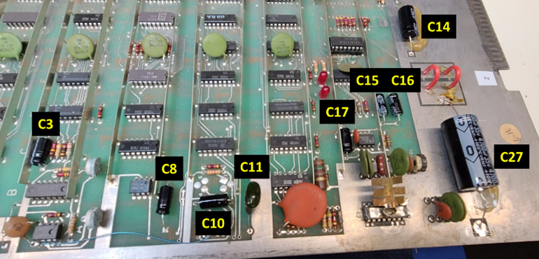
Figure 51: Changed out capacitors on main PCB.
One thing you’ll notice on the ND PCB is the large runs of metal sticking up above the board along the rows of chips. These are the bus lines, and you can use them to easily probe power and ground for each column of chips. I used a multimeter (set on resistance) to check for weak points/shorts in each column, but everything seemed ok (or at least, ok enough for a power-up test).
Edge Connector
The next thing to repair was the edge connector. You’ll see a lot of advice and videos online on this topic, as it was fairly common on the older boards for burning to occur on power pins (think: drawing too much current through a pin, bad contacts, oxidized pins, etc.). Pretty typical, but not too pretty:
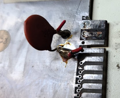
Figure 52: Toasty power and ground pins on the edge connector.
To get mine in shape, I took the following steps:
- Gently used a small wire brush wheel on a Dremel and go over all the contacts, to clean off the oxidation and crud
- Clean the edge with Q-tips and isopropyl – just to get things a basic level of clean
- Used a small metal file to flatten out the unevenness in the PCB on the burned area as much as possible.
The bad pins (A/1, B/2) are power (of course), and are the same thing on the parts side and the solder side – so A and 1 are Ground, B and 2 are a power line. This meant I was able to do the next step very cleanly….
- Apply copper tape with a self-adhesive backing to both pins, folding the tape over the edge of the board and around to the other side. You can see it in the following picture:
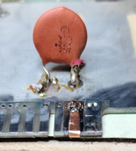
Figure 53: Adding foil to the first pin. Note how it wraps around the PCB!
- Trim the copper to ensure it only covers the original pad area, then use a little solder to connect the copper foil to the PCB at the top of each pad. Do this on both sides, obviously.
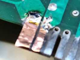
Figure 54: Close-up of pins with new copper foil in place. Sorry it’s out of focus!
- Use non-metallic nail polish as simple brush-on insulation at the top where you’ve done the soldering:
Figure 55: Using nail polish to provide a little extra insulation.
Missing Program ROMs
The next step in this board repair was to figure out the missing ROM situation. I initially assumed I would just be able to pick a few spares out of my stash, burn them, stick them in, and we’d be good. Sadly, not so much – the ones Atari used were mask roms at D2 (Atari part 006569) and E/F2 (Atari part 006570):
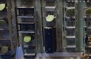
Figure 56: Location of Missing ROMs (upper left)
The problem with these missing is that you can’t really get replacements (easily) for mask roms of this vintage, and the pinouts of these roms wasn’t quite the same as the more standard eproms of the day (ala 2708, 2716, etc.). On top of this, the key control lines on the mask rom are active high, whereas for the more standard ones they are active low. I thus went and designed a very simple PCB using some IC sockets, two modern 2716 eproms, and a 7404 inverter chip. The pin mapping/wiring is shown in the table below:
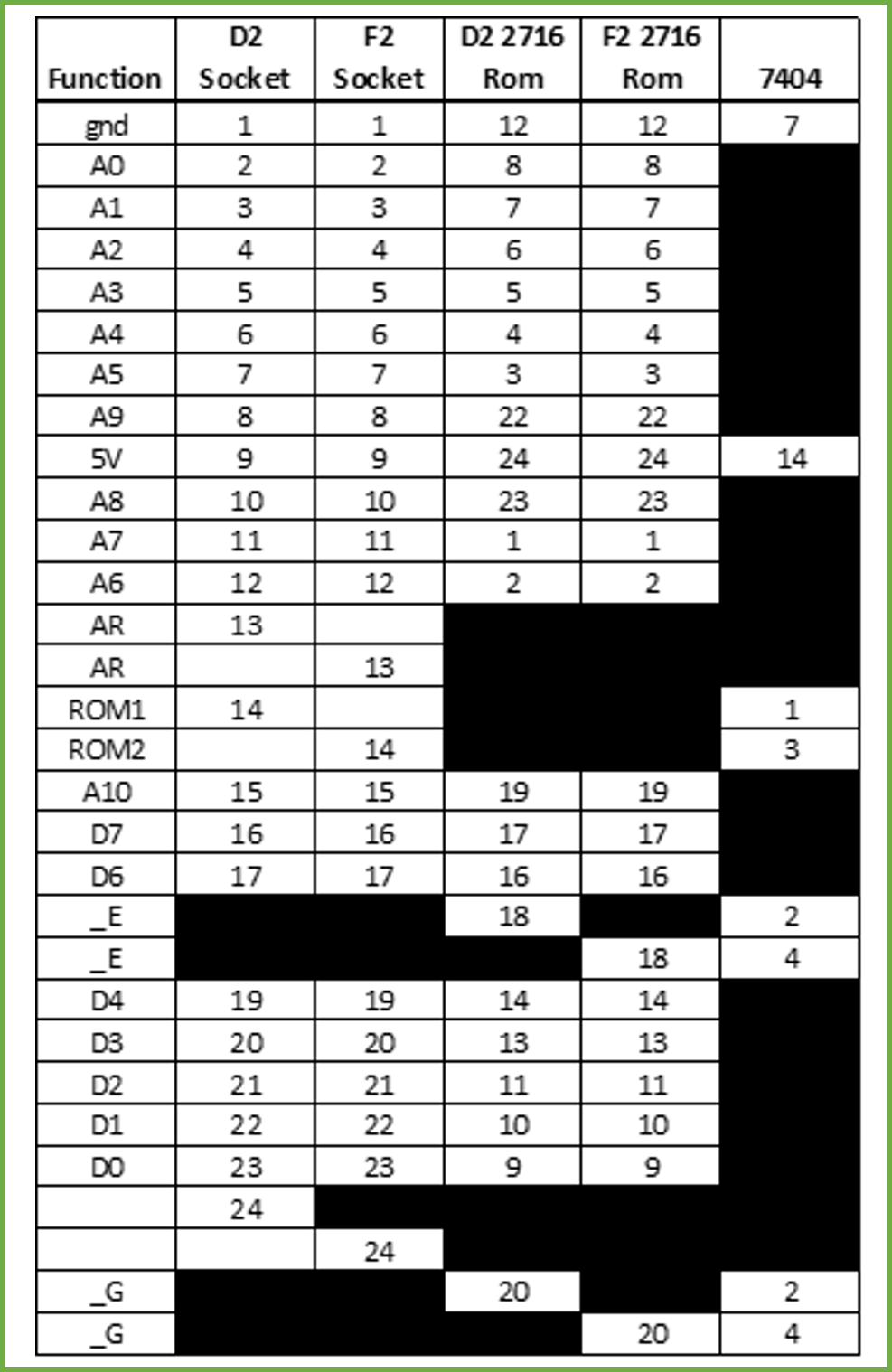
Figure 57: Mapping of mask rom IC socket pins to 2716 eprom pins, with 7404 inverter for control lines.
The layout looks like:
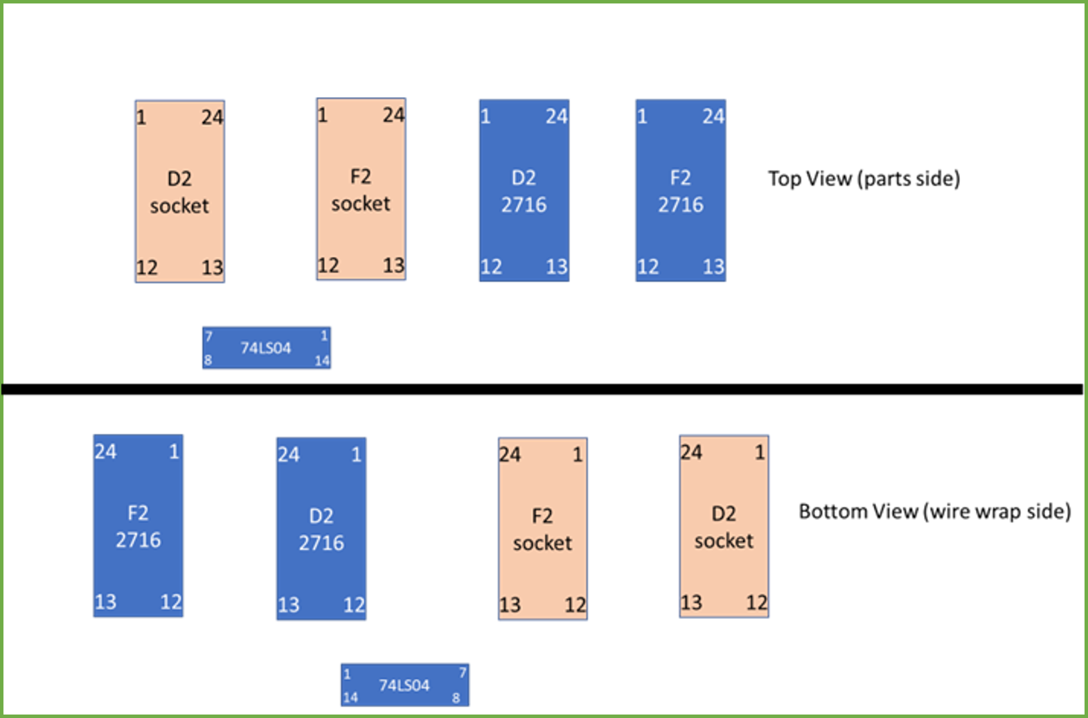
Figure 58: Simple diagram showing the part layout/pin numbering for the rom board.
I used a wire wrap tool and a piece of 10×8 cm perfboard (similar to this one, but different size). First I aligned two wire-wrap sockets on my board with the ones on the ND PCB, and soldered those to the perfboard. Next, I placed sockets for the two new eproms to align with those (for ease of wrapping), as well as sticking a socket for a 7404 below, and soldered those down to hold them in place. Next I labeled each chip/socket location using a labeler (so I wouldn’t get confused), and a applied wrap-wrap labels (like this) to the bottom of each IC socket. If you’ve never used those labels, they help (a lot!) in keeping you from miscounting the pins as you are wiring the board.
I carefully wired the board using the table, keeping to a simple standard of red power lines, black ground lines, blue data lines, and white address/control lines. Once I finished the connections I checked them with a meter (to find mistakes/shorts) and corrected any badness (I only made one mistake this time). I also went back and added 0.01uF bypass caps across the power pins on the eprom sockets. I also threw a couple IC sockets on the end of the wire wrap pins that go into the ND PCB so as to keep the long leads aligned and make it easier to insert. The PCB came out ok, though not exactly beautiful:
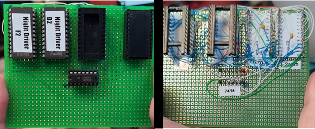
Figure 59: ROM adapter board – parts and wire-wrap side.
I downloaded the images from the web, blanked two 2716 eproms (in a UV eraser), then burned them with my Willem GQ-4X burner. The whole set of ND roms is here, if you need them. And then I mounted the whole thing on the ND board:
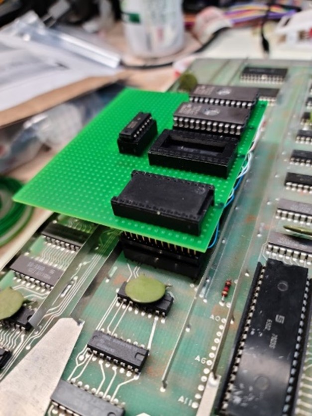
Figure 60: ROM adapted PCB mounted on the ND board. She’s no beauty queen, but not too bad given I didn’t want to wait for a PCB to be etched…
Two more things were missing here: labels, and strain relief. If you’re new to EPROMs you might not know that you need to actually cover up those windows on top of the device – otherwise, over time, it is entirely possible that light exposure may end up erasing/flipping a bit or two and that will stop your board from running property. I used to use black electrical tape for this, but found that I like it much better when I could properly label the roms – thus, I now use Avery laser printer labels, download the template to Word, fill it in, print, trim them down, and stick them on. It works well, the labels don’t come off, and I’m just happier about it.
On the strain relief side, what you’ll find is these little add-on boards have a bad tendency to fall off or do bad things if they aren’t glued down or strain relieved in some manner. In this case we have those long power rail metal strips, which make a great place to feed a wire tie through and secure. The final product looked like:
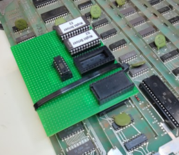
Figure 61: Rom board with tie-down and labels, in place, on the ND PCB. Not bad!
Ready for testing, no? Oh, yeah, what about powering this board…
PCB Power Conversion
Atari PCBs of this era tended to use a transformer and a few diodes in the base of the machine, then fed the power to the PCB for further rectification and regulation (e.g. turning the 18VAC signals into +5VDC and +12VDC, etc.). This is fine, and you can rebuild this sort of setup, but my machine was missing the transformer/diode bit, and transformers tend to be pricey nowadays because they involve copper, steel, etc. and so many systems have moved to switching supplies. What to do? I decided to leverage a PC power supply (see the other section) to provide the +5VDC and +12VDC, which has a number of advantages – not the least of which is that it removes the need for the regulation onboard the PCB. Why would you care about that? Those old-school TO-3 case regulators run hot, and that requires the heat sink AND tends to cook the PCB. The circuits Atari used also included a giant power resistor, which again, gets hot and doesn’t do good things for the board.
Given the change, I had to modify the onboard power circuits as follows:
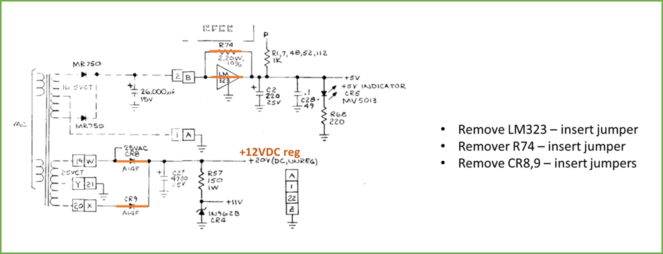
Figure 62: Modifications to power circuits on the Night Driver PCB
For the 5V circuit, I bypass the LM323 and the R74 – they are both now unnecessary, and this kills a ton of heat. I leave the filter caps and the rest in there, though, to smooth the 5V source going in and filter noise. For the 12V, I bypass the two diodes (don’t need rectification here anymore). I leave R57, the 11V Zener (it’s fine), and the filter caps.
Now, you might be saying: very clever, and the 5V makes sense – but hooking up 12V at pin 19/W/20/X isn’t going to get you 20VDC unregulated! Of course, you are right, but if you poke around the ND board you realize, like many games, that circuit is just used for the audio amps, and 12V will work just fine.
The jumpers I used were 16 gauge solid, and the PCB looks as follows:
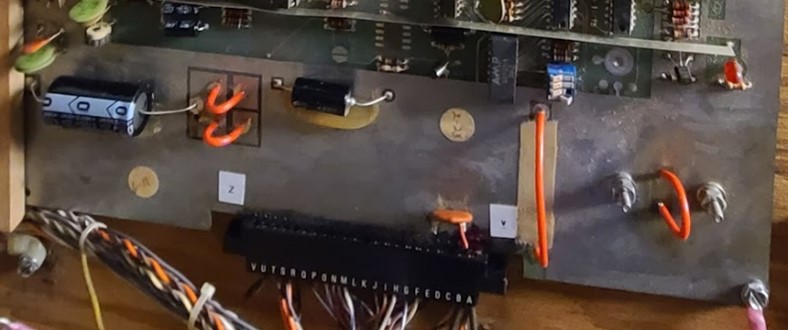
Figure 63: Power jumper bypasses in place. Only do this if you plan to hook up an external 5V/12VDC source!
That was all I had to do to convert the PCB. See the power supply section for details on the rest of the power conversion.
Testing
My test bench leverages a simple “bar top” arcade cabinet with a switching power supply, VGA screen, RGB to VGA converter, a speaker, and so on, and has a jamma interface. Of course, ND isn’t jamma, uses a steering wheel, and has a composite video out, thus most of that rig wasn’t useful here. Nevertheless, I went and built a simple adapter with a split fingerboard so my jamma rig could supply the 5V and 12V and I could use the speaker. I hooked up a bunch of the other stuff as I could, but I don’t think all is right there (have to double check some of it). To the board side of the adapter I attached a simple RCA cable so it could be hooked up to an external monitor with a composite input.
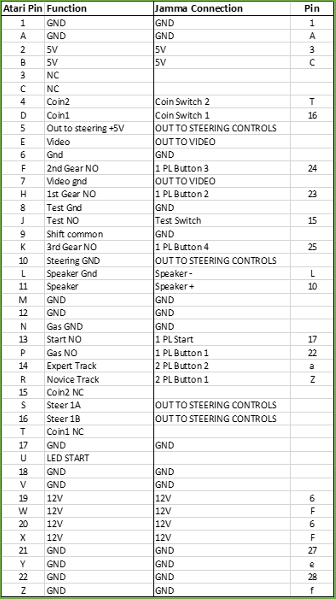
Figure 64: Jamma adapter mapping. The control mappings aren’t quite right, thus at some point I’ll have to go back and figure that out.
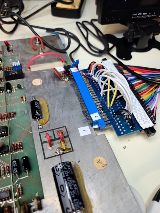
Figure 65: Goofy semi-jamma adapter. Note how I tend to label everything, including the edge connector and how it fits onto the PCB (when there is little or no keying). You never, ever want to plus these things in upside down or backward, as you can short things out. Labeling helps avoid issues.
But what monitor? I’ve got slews of them, but didn’t have one handy that took composite input and were easy to deal with (and I had already set aside the 22V1001). I wanted something small, light, bulletproof to use for this and other composite boards. Fortunately, we live in an era where everything and anything is available, usually overnight if you are lucky. I picked up a very inexpensive backup display that can be used in cars. It is a 7” screen, takes a composite input, comes with a little stand, and is powered by a 12V source. Good stuff, and super light/portable! I hooked it up to a cheap 12V adapter, and all ready to go!
Putting together the PCB, test monitor, and jamma adapter/rig on the workbench, we were ready to go and powered up:
Figure 66: ND PCB, ROM adapter board, jamma adapter, test monitor, and jamma test rig (to the right, out of the photo). Note that I did the testing here at about the same time I labeled and strain-relieved the rom board, so don’t be confused by the lack of those aspects.
Taking a closer look at the monitor, I couldn’t have been happier:
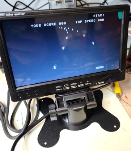
Figure 67: Looks like Night Driver to me!
I did actually hook up a few of the controls to my test rig via the jamma adapter, including the test switch pin on the edge connector. Pushing the button on my rig (e.g., flipping the test switch) gave me this on the monitor:
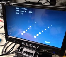
Figure 68: Test screen on first power-up. Looks pretty good!
Which looks a lot like the test screen in the manual (though seemingly cut off on the top):
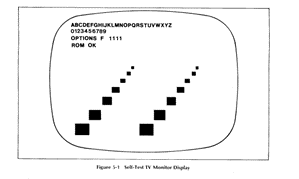
Figure 69: Self-test in the manual. Only difference seems to be the option settings (the dip switches) and the alphabet at the top of the screen.
I wouldn’t call this a complete shake-down of the PCB and its functionality, but to do that, I’d really need to hook up the wheel/optos and such. I thus set aside the PCB for further testing once I got it into the cabinet and hooked up to the rest of the stuff.